19.3 “High Performance PRAM Cell Scalable to sub
advertisement
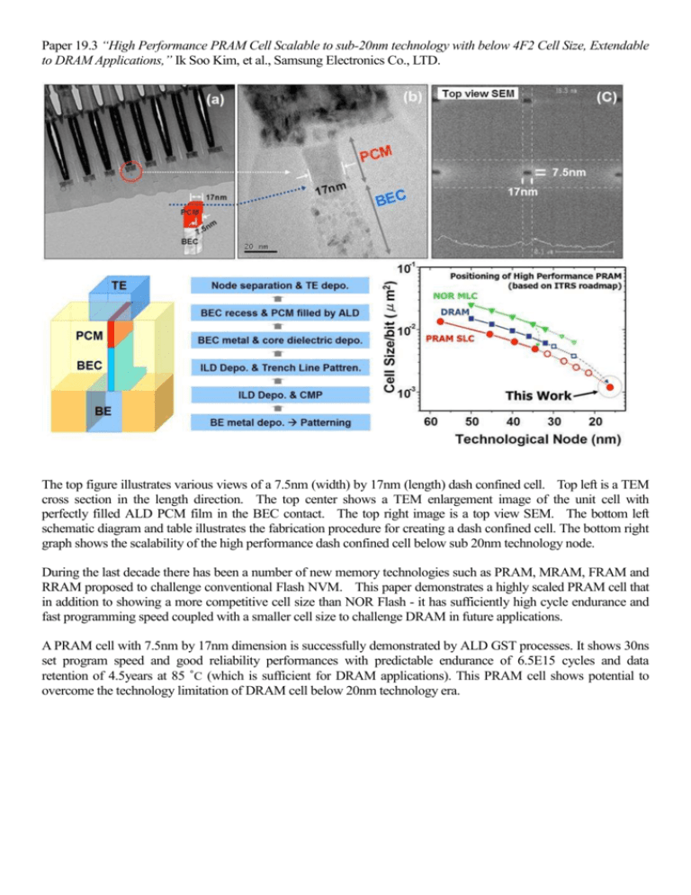
Paper 19.3 “High Performance PRAM Cell Scalable to sub-20nm technology with below 4F2 Cell Size, Extendable to DRAM Applications,” Ik Soo Kim, et al., Samsung Electronics Co., LTD. The top figure illustrates various views of a 7.5nm (width) by 17nm (length) dash confined cell. Top left is a TEM cross section in the length direction. The top center shows a TEM enlargement image of the unit cell with perfectly filled ALD PCM film in the BEC contact. The top right image is a top view SEM. The bottom left schematic diagram and table illustrates the fabrication procedure for creating a dash confined cell. The bottom right graph shows the scalability of the high performance dash confined cell below sub 20nm technology node. During the last decade there has been a number of new memory technologies such as PRAM, MRAM, FRAM and RRAM proposed to challenge conventional Flash NVM. This paper demonstrates a highly scaled PRAM cell that in addition to showing a more competitive cell size than NOR Flash - it has sufficiently high cycle endurance and fast programming speed coupled with a smaller cell size to challenge DRAM in future applications. A PRAM cell with 7.5nm by 17nm dimension is successfully demonstrated by ALD GST processes. It shows 30ns set program speed and good reliability performances with predictable endurance of 6.5E15 cycles and data retention of 4.5years at 85 ˚C (which is sufficient for DRAM applications). This PRAM cell shows potential to overcome the technology limitation of DRAM cell below 20nm technology era.
