Termination - LVCMOS
AN-845
APPLICATION NOTE
Introduction
This application note provides examples of high speed LVCMOS driver clock drivers. For high-speed LVCMOS drivers, general
rules for high-speed digital board design must be followed. Proper termination is required to ensure signal quality and
Electro-Magnetic Interference (EMI) reduction.
There are many different termination schemes for single-ended LVCMOS drivers. This application note discusses parallel
termination, AC termination and series termination. The following termination approaches are only general recommendations
under ideal conditions. Board designers should consult with their signal integrity engineers or verify through simulations in their
system environment.
Parallel (DC) Termination
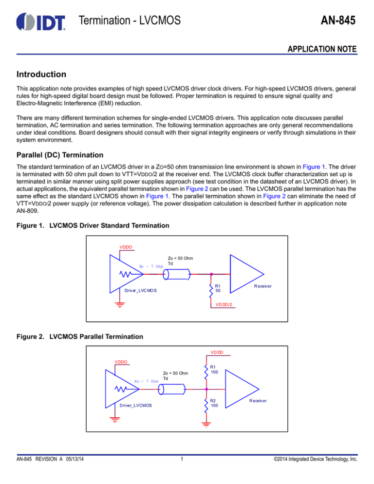
The standard termination of an LVCMOS driver in a ZO=50 ohm transmission line environment is shown in Figure 1. The driver
is terminated with 50 ohm pull down to VTT=VDDO/2 at the receiver end. The LVCMOS clock buffer characterization set up is
terminated in similar manner using split power supplies approach (see test condition in the datasheet of an LVCMOS driver). In
actual applications, the equivalent parallel termination shown in Figure 2 can be used. The LVCMOS parallel termination has the
same effect as the standard LVCMOS shown in Figure 1. The parallel termination shown in Figure 2 can eliminate the need of
VTT=VDDO/2 power supply (or reference voltage). The power dissipation calculation is described further in application note
AN-809.
Figure 1. LVCMOS Driver Standard Termination
VDDO
Ro ~ 7 Ohm
Zo = 50 Ohm
Td
R1
50
Dr iver _LVC MO S
R eceiver
VD DO /2
Figure 2. LVCMOS Parallel Termination
VD DO
VDDO
Ro ~ 7 Ohm
Zo = 50 Ohm
Td
R2
100
D river_LVCMOS
AN-845 REVISION A 05/13/14
R1
100
1
R eceiver
©2014 Integrated Device Technology, Inc.
AN-845
AC Termination
The LVCMOS driver AC termination in a 50 ohm transmission line environment is shown in Figure 3. The majority of load current
is drawn during transient region (i.e. rising edge and falling edge). This termination consumes less power than the parallel
termination. The proper value of capacitor C1 depends on the trace delay and capacitance of the transmission line. Some PC
board layout or simulation software tools provide a feature of calculating the transmission line capacitance by entering the trace
information (see References, [1]).
Figure 3. AC Termination
Zo = 50 O hm
Ro ~ 7 Ohm
LVC MO S_D river
R1
Zo =50
Receiver
C1
Series Termination
Series termination is a popular termination scheme for LVCMOS drivers. Figure 4 shows a simple series termination for LVCMOS
drivers with output impedance of 7 ohm. The Power Dissipation of this termination scheme is described in a separate document.
The typical output impedance RO of a high speed LVCMOS driver is approximately 7 to 16 ohms (some parts might have different
RO value. Refer to datasheet for the output impedance). For example, RO=7 ohm, the closest series resistor value, RS, can be
calculated as follows:
RS = ZO - RO = 43 ohms
In the Figure 4, the footprint for optional series resistor R3 or optional capacitor C1 at the receiver input is recommend for
adjusting edge rate or overshoot if necessary.
Figure 4. One-to-One LVCMOS Series Termination
Zo = 50 O hm
Ro ~ 7 Ohm
RS
R3
43
0
LVCMOS Driver
C1
Receiver
SPARE
When the number of drivers is not equal to number of receivers as shown in Figure 6, the series resistor value RS is calculated
as follows:
RS = ZO - (RO x M)/(N)
where N = number of driver; M = number of receiver
This configuration assumes that all the trace delays and load conditions are equally matched.
TERMINATION - LVCMOS
2
REVISION A 05/13/14
AN-845
For example, one driver driving 2 receivers as shown in Figure 5, with N=1and M=2, the series resistor is calculated to be RS =
36 ohms. The trace delays Td on TL1 are equal. The loading conditions on both receivers should also be equal.
Figure 5. Series Termination for One LVCMOS Driver Driving Two Receivers
QA0
Ro ~ 7 Ohm
Zo = 50 O hm
Td
R S1
36 Ohm
TL 1
8701
Receiver
Zo = 50 O hm
Td
R S2
36 Ohm
TL 2
Receiver
For 5 drivers driving 6 receivers, the closest series resistor can be calculated as follows:
N=5, N=6, ZO=50 Ohms, RO =7 ohm
RS = 50 - (7 x 6)/5 = 41.6 ohm
The result above is straight from calculations. The closest available resistor value should be chosen.
Figure 6. Tie N Outputs Together to Drive M Receivers
Q1
Ro ~ 7 Ohm
Zo = 50 O hm
Td
R1
LVCMOS D river
RS
TL _1
Receiver1
Q2
Ro ~ 7 Ohm
Zo = 50 O hm
Td
R2
LVCMOS D river
RS
TL _2
Receiver2
Zo = 50 O hm
Td
RM
QN
Ro ~ 7 Ohm
RS
TL _M
ReceiverM
LVCMOS D river
REVISION A 05/13/14
3
TERMINATION - LVCMOS
AN-845
PC Board Layout with Option of Multiple Termination Scheme
For signal integrity, take the necessary precaution and follow the high-speed digital design rules as much as possible. In most
cases, the board design cannot fully comply the high-speed design rules due to constrains on the board environment, e.g. space
available, cost, etc. There is always some unknown parameters or interference in the system environment. The signal quality
can only be optimized through the experiment; one termination scheme may work better then the other. While capturing a
schematic for PC Board layout, if there is space available, it is recommended to provide options to choose different termination
schemes. Figure 7 shows an example schematic for a PC board footprint that provides an option of choosing various types of
terminations.
Figure 7. PC Board Layout Provides Footprint to Choose Various Termination Options
VDD O
R1
SPARE
Ro ~ 7 Ohm
RS
43
R3
Zo = 50 O hm
LVCMOS_Dr iver
0
R2
Receiver
SPARE
C1
SPARE
References
[1] Kaufer, Steve, Crisafulli, Kellee, Terminating Trace on High-Speed PCBs, Printed Circuit Design, March 1998
[2] Dr. Johnson, Howard, Dr. Graham, Martin, High-Speed Digital Design, A Handbook of Black Magic, Prentice Hall, 1993
TERMINATION - LVCMOS
4
REVISION A 05/13/14
Corporate Headquarters
Sales
Tech Support
6024 Silver Creek Valley Road
San Jose, CA 95138 USA
1-800-345-7015 or 408-284-8200
Fax: 408-284-2775
www.IDT.com
email: clocks@idt.com
DISCLAIMER Integrated Device Technology, Inc. (IDT) and its subsidiaries reserve the right to modify the products and/or specifications described herein at any time and at IDT’s sole discretion. All information in
this document, including descriptions of product features and performance, is subject to change without notice. Performance specifications and the operating parameters of the described products are determined
in the independent state and are not guaranteed to perform the same way when installed in customer products. The information contained herein is provided without representation or warranty of any kind, whether
express or implied, including, but not limited to, the suitability of IDT’s products for any particular purpose, an implied warranty of merchantability, or non-infringement of the intellectual property rights of others. This
document is presented only as a guide and does not convey any license under intellectual property rights of IDT or any third parties.
IDT’s products are not intended for use in applications involving extreme environmental conditions or in life support systems or similar devices where the failure or malfunction of an IDT product can be reasonably
expected to significantly affect the health or safety of users. Anyone using an IDT product in such a manner does so at their own risk, absent an express, written agreement by IDT.
Integrated Device Technology, IDT and the IDT logo are registered trademarks of IDT. Product specification subject to change without notice. Other trademarks and service marks used herein, including protected
names, logos and designs, are the property of IDT or their respective third party owners.
Copyright ©2014 Integrated Device Technology, Inc.. All rights reserved.


